RTL DESIGN · FPGA · VERIFICATION

Digital hardware.
Visible evidence.

I'm Karan Kumar, an ECE final-year student at IIIT Bhagalpur. I build digital hardware and investigate its behaviour through simulation, formal safety checks, and FPGA experiments.

SystemVerilog / VerilogSimulation + formalFPGA integrationCMOS fundamentals

INTERACTIVE SILICON EXPLORER

Follow a signal through the silicon.

Tap a stage, change the inputs, and see how a simple logic idea connects to a complete hardware system.

TRANSISTOR-LEVEL IDEA

CMOS inverter

Toggle the input. A simplified PMOS/NMOS model shows why the output changes in the opposite direction.

INPUT A 0
CMOS PAIR INVERT
OUTPUT Y 1

Input A is low, so the output is high.

SELECTED ENGINEERING WORK

Four projects. Different layers.

From transistor-level simulation to RTL verification and a complete FPGA system.

02 / RTL + UVM

AXI4-Lite Countdown Timer

SystemVerilog · UVM 1.2

A memory-mapped countdown timer with CONTROL, RELOAD, COUNT, and STATUS registers. A UVM testbench drives AXI4-Lite transactions, monitors completed transfers, and checks expected register and timer behaviour in a scoreboard.

Reset recoveryIncomplete write cancelled
and normal traffic resumed
Timer behaviorCountdown, busy state,
interrupt and clear checks
Clean regression120 UVM info messages
0 warnings, errors or fatals

Simulation-based verification. This regression is not a formal proof or a complete AXI compliance certification.

Try the timer

Set a short reload value, start the countdown, and watch the status and interrupt.

Interactive demo
COUNT0
STATUSIDLE
IRQLOW

Ready. Choose a reload value and start.

Show UVM-inspired activity trace
  1. Ready: waiting for a timer start.

Browser-side JavaScript model for learning. It does not run the SystemVerilog RTL or Vivado UVM testbench.

03 / FPGA SYSTEMS

AES-128-GCM image security

ZCU104

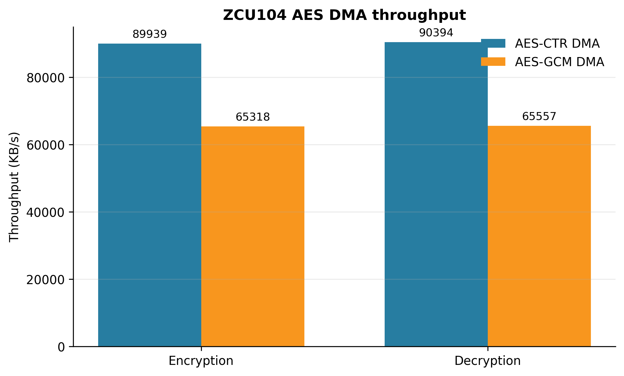
A Verilog accelerator integrated with AXI4-Stream, AXI DMA, and Cortex-A53 software. The project checks FPGA ciphertext and authentication tags against Python AESGCM and tests modified-ciphertext rejection.

  • Hardware/software co-design
  • Independent reference checks
  • Documented timing and resource results

An engineering research prototype. Results and limitations are documented separately for its baseline and protected-chunk architectures.

Measured encryption and decryption throughput comparison of the CTR-DMA and GCM-DMA architectures.
Measured FPGA resultsPreserved CTR-DMA and GCM-DMA throughput comparison. The results document explains measurement conditions. Read the source evidence ↗
04 / CMOS DESIGN

CMOS 1-bit full adder

gpdk180

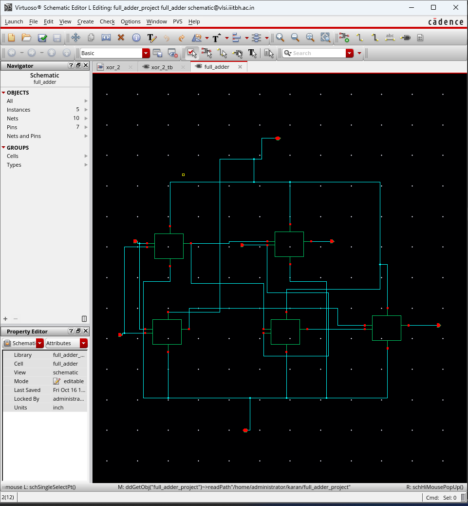
A hierarchical static CMOS full adder in Cadence Virtuoso, simulated with Spectre. The documentation includes all eight input combinations, waveforms, and output-load characterization.

  • 180 nm generic process
  • 1.8 V nominal supply
  • Schematic-level simulation

Scope: schematic simulation and characterization. Physical layout, DRC, and LVS are outside this project.

Cadence Virtuoso screenshot of the hierarchical CMOS full-adder schematic.
Circuit design evidenceHierarchical full-adder schematic in Virtuoso. Schematic-level work; no layout, DRC, or LVS result is implied. Read the source evidence ↗

EXPLORE THE IDEA

An image. A key. One changed byte.

Try authenticated encryption, then challenge it. This browser lab is separate from the FPGA implementation and its measurements.

AES-128-GCMLocal browser processing · no image upload

Choose an image or use the sample. Encrypt its file bytes, recover the original, and flip one ciphertext bit to test authentication.

01 Original

Your image starts here.

Nothing selected

02 Ciphertext + tag

Choose an image, then encrypt.

Bytes shown as hexadecimal

03 Recovered

Released only after authentication.

Awaiting verification

Enable JavaScript to try the lab. The project evidence above remains available.

What happens under the hood?

The Web Crypto API generates a fresh 128-bit AES key and random 96-bit IV for each encryption. GCM appends a 128-bit authentication tag. Decryption must authenticate before this page displays a recovered image. The tampering test flips one ciphertext bit in a copy; the original encrypted bytes stay available for another valid decryption.

This lab encrypts compressed image file bytes, not the FPGA project's raw pixel stream. Keys and images stay in page memory; resetting clears this lab's references. This is a learning demo, with no key export or persistent storage.

IV
Not generated
Tag
Not generated

HOW I APPROACH THE WORK

Make the claim inspectable.

01

Define the contract

State transfer rules, reset behaviour, supported parameters, and the assumptions around the design.

02

Challenge the behaviour

Exercise boundary conditions, stalls, and resets. Compare outputs with a separate reference model.

03

Keep the evidence

Link results to test plans, configurations, and scripts so readers can inspect and reproduce the checks.

ABOUT ME

Building depth in
digital hardware.

My interests span RTL design, functional and formal verification, FPGA acceleration, and secure digital systems. My projects connect digital logic fundamentals with practical tool flows.

Open to internships, entry-level opportunities, and engineering collaboration.

Project toolkit

RTL & verification
SystemVerilog, Verilog, Icarus Verilog, Yosys/SMTBMC, Z3
FPGA development
Vivado, Vitis, AXI4-Stream, AXI4-Lite, AXI DMA
Circuits & software
Cadence Virtuoso, Spectre, Python, C/C++

Tools used in the linked projects; project documentation defines the tested scope.

Project evidence